N2PK Vector Network Analyzer
An inexpensive Vector Network Analyzer of a Lab qualitymakarov.ca
Dual Detector VNA board v5 build info
VNA v5.x dual detector board construction hints and tips
This page has information specific to the Dual detector VNA v5.x family boards, as well as links to the VNA schematics and Bill of Materials. I will be updating it as new information becomes available, but on this page it will be presented in no particular order.
The v5 PCB is the result of logical development of the project and trends in the computer industry. Parallel ports are becoming less common in portable computers which are often used to host the N2PK VNA software, and USB type interfaces now dominate. The new VNA PCB with USB support meets these demanding requirements.


If you are new to the project, please visit Paul N2PK's WEB site first and read the original project documentation. Then return and read the VNA materials on this WEB site, specifically previous generation board revision v4.x information. Understanding the project background and history will help you set the right expectations for a VNA project and answer many of the questions that you may have.
It is also recommended to subscribe to N2PK-VNA Yahoo group that has tons of valuable information on how to build and use the VNA.
Specification
The Specification is given as a refresher because it is mostly the same as for the previous v4.x PCB generation. The only real difference is replacement of the parallel port with USB one.| Frequency range: | 0.05...60MHz | ||
| Dynamic range: | 120dB | ||
| Detector ports input impedance: | 50 Ohm | ||
| Detector ports Return Loss: | 30 dB | ||
| Detector ports max input power: | +10dBm | ||
| Detector ports ADC resolution: | 24 bit | ||
| RF DDS port max output power | +4 dBm | ||
| Number of detectors: | 2 | ||
| Detector Resolution Bandwidth: | Selectable from 7Hz to 3.4kHz | ||
| Features: | VNA, Dual RF signal/sweep generator, Vector Voltmeter | ||
| PC interface: | USB v2 | ||
| Power consumption: | +5V @250mA, +10V @50mA | ||
| Size: | 6.3x2.7'' (159x69mm) |
Summary of changes
Schematics:
- - DDS source and Detectors: no change
- - PC interface: The Parallel port interface has been replaced with a USB interface. No more support for the parallel port.
Cost of parts: No significant change. All parallel port support elements have been removed, but inclusion of the USB support compensated for the cost saving. However, if you consider the overall cost of a VNA project, the v5.0 board still gives some savings, because the new board has the USB interface integrated. Previously the USB interface had to be purchased and built separately.
Efforts: The new v5.0 board is more integrated and easier to assemble. All PC interface wiring has been eliminated and the board only requires wiring of the power supply and the front panel RF connectors. The majority of tedious connector crimping job has gone.
Portability: The new v.5 PCB was designed to allow the second detector be separated and mounted separately to achieve a better isolation and wider dynamic range - see the picture below. The two pieces then can easily be connected with a 5-wire harness or a flat cable.

Alternatively, the second detector piece can simply be removed and a single detector VNA built if the builder decides to reduce cost and efforts. The second detector can be then assembled and added at a later time.
The new board has J702 header extension which controls miscellaneous external devices. Examples are: step attenuator, S-parameters Test Set, RF-IV Sensor. The lines are under control of the software which toggles them on and off as required by the current operating mode. For the basic VNA functionality this extension is not used.
Design of the USB interface, USB chip firmware, and Windows drivers was done by Dave Roberts, G8KBB. Schematically it is the same circuit which was previously offered as a standalone USB interface PCB. It has now become an integral part of the v5 N2PK VNA dual detector board.
The USB interface receives power from the USB port. Even if the VNA is not powered on, the USB chip begins to work as soon as the VNA is connected to the PC. This is for example used to initialize the USB chip for the very first time. Also, the USB chip senses the VNA power and if the user forgets to turn the VNA power on and tries to make a calibration or a scan, a warning message is displayed telling the user the VNA is switched off.
Constructions details
A USB 2.0 quality cable has to be used to connect the VNA to the PC. It is also advisable to place a snap-on ferrite choke on the USB cable close to the VNA, or purchase a USB cable that already has one. This is especially important in places like RF shacks with a higher level of ambient RF power. This will reduce chances of RF getting into the VNA box via USB circuit causing glitches and distorting measurements.
Note the USB connector casing is NOT directly connected to VNA ground and should NOT touch VNA enclosure. Per USB specification the casing is grounded via a safety circuit consisting of a high voltage capacitor and a 10MOhm resistor in parallel - see board v5.x DDS section schematic.
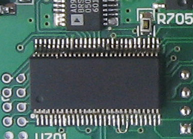 | Cypress USB chip datasheet is specifying the pin 21 as Not Used. But it turned out it must be connected to Ground, or the chip will not work. If your board is of v5.0, please connect pin 21 of the USB chip U701 to ground. In this picture I connected it with a short strand of wire to pin 19 (which is also Ground), but pin 21 can be connected to any nearby Ground plane. |
When mounting the board in the enclosure use all 6 mounting holes to reduce board flexing. The voltage reference ICs in the detectors are sensitive to mechanical stresses (this is common for the ICs in the class) and under stress change the output voltage on microvolt level, which is however enough to produce an offset in ADC readings.
Use a 8-pin 0.1'' 2-row SIP header connector for J702. It can be also constructed from a longer 1-row SIP connector by cutting two 4-pin pieces out of it. As noted above, J702 has control lines for optional hardware. Even if you are not considering using it now, later you may want to use the extension and the presoldered PCB header J702 would come handy.
Board revision v5.1 details
Beginning August 2009 new board revision v5.1 will be supplied. The updated layout has pin 21 of the USB chip grounded. No other changes were introduced.
Board revision v5.2 details
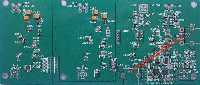
Beginning May 2010 new board revision v5.2 will be supplied. The updated layout has a provision to install the USB connector at the shorter edge of the PCB. So the builder can now choose to solder the USB connector at either the long or short PCB edge, depending on how it is planned to mount the board in the box. When modifying the layout to add the second USB connector, there was no space available to route the power lines coming out from the USB, so if the USB connector is installed at the shorter edge of the board (J701a), two power wires must be soldered as shown in the picture. If the USB connector is installed at J701 location, no extra power wires are required. No other changes were introduced to the layout or BOM compare to the previous version of the board.
Software
1. User interface. All N2PK VNA software that supports USB will work with the v5.x boards. Examples are myVNA, VNA4Win. DOS-based programs from Paul N2PK can not work with the v5 board because they use parallel port type of interface which is not supported by the v5 board.
2. USB chip firmware and Windows driver package. The package consists of two parts:
- USB chip Identity. Has to be programmed into to the chip during USB chip initialization when the interface gets powered for the first time after the board is built. The VNA firmware itself is downloaded to the USB chip every time it is plugged into the PC. Follow the USB interface documentation from Dave G8KBB to program the correct ID into the chip using USBConfigure
- -Windows drivers. Have to be installed after the USB chip Identity programming step. Follow the USB interface documentation from Dave G8KBB to install the drivers.
Dave has done a great job and wrote the drivers to support all existing v4.x boards as well as the new v5.x ones. When the VNA is plugged in, the driver can recognize which board version the VNA is based on and switch itself to the appropriate mode.
Downloads
| Schematics | Connection diagram | ||||
| Bill of Materials | High res picture Top | ||||
| Assembly drawings | High res picture Bottom |
Boards and parts availability
To check PCB availability click here. You will be redirected to the page that has latest PCB availability information.
Parts can be purchased from DigiKey using the BOM from the Downloads section above.
Credits
I would like to thank the people, who helped me to make the new v5 board available, for their contribution. Here is the names list in alphabetical order:
- Dave Roberts, G8KBB, for the USB hardware design, USB firmware and driver development, software support, and reviewing the article;
- Larry Molitor, W7IUV, for being the first live user of the v5 VNA and giving it a thorough test in real conditions;
- Paul Kiciak, N2PK, for reviewing the article and providing valuable comments.
Please feel free to direct your questions or comments to the email address below.
Contact:  miv@makarov.ca